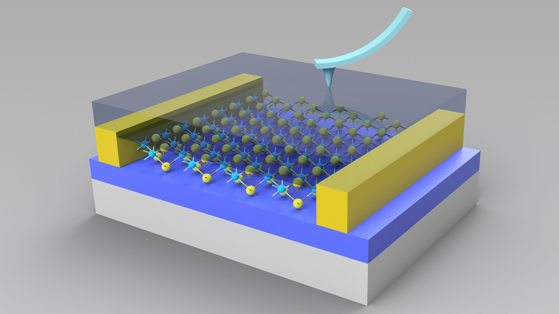
Recent research from the University of Nebraska-Lincoln may help future engineers of digital components get two (or more) for the space of one.
A team of physicists has demonstrated a reversible method for altering the electronic properties of a nanoscopic material, pointing the way toward merging several hallmark functions of modern electronics into a single component.
The approach might ultimately allow a 2-D material to shift from digital processing to power conversion to light-triggered applications. That versatility, in turn, could give engineers additional options for scaling down electronics by squeezing more functionality into one device.
Xia Hong and her colleagues started with an atomically thin slice of molybdenum disulfide, or MoS2, a chemical compound whose semiconducting properties resemble those of industry favorite silicon. They then overlaid the MoS2 with a polymer featuring ferroelectricity – the ability to reverse the alignment of its separated positive and negative charges, or polarization, by applying an electric field to it.
The researchers discovered that they could radically reconfigure the electronic behavior of the MoS2 by selectively applying voltage across the polymer to dictate the direction of its polarization.
When Hong’s team aligned the polymer’s positive or negative charges either toward or away from the layer of MoS2, the latter’s electric current flowed freely in both directions and corresponded to the amount of voltage applied. In that state, the MoS2 played the role of transistor, a signature component of digital processing that releases and suppresses electric current to speak the binary language of 1s and 0s.
But when the team polarized the polymer in a different way – creating two domains of vertically oriented but oppositely aligned polarizations – the underlying MoS2 adopted a new identity. Rather than acting as a transistor, the MoS2 became a diode, allowing current to flow in one direction but resisting its movement in the other when subjected to different polarities but the same amount of voltage.
Among their many purposes, diodes convert the two-way flow of alternating current – used in powering homes and other structures – into the one-way transmission of direct current that powers virtually any technology containing a battery. They also reside at the heart of many light-powered and light-producing devices, from solar cells to LED displays.
The MoS2 maintained its transistor and diode states even when the voltage was removed, Hong said. That quality, combined with the technique’s low voltage requirements and nanoscopic scale, led her to describe it as “very promising” for low-power technological applications. The mechanical properties of the atom-thin superconductor and ferroelectric polymer, she said, could prove especially suited to the sort of flexible electronics found in wearable technology.

“This is not just a performance enhancement,” said Hong, associate professor of physics and astronomy. “It’s really (about) creating a new type of multi-functional device.”
Hong said the approach’s reversibility might make it preferable to the decades-old semiconductor treatment process known as doping, a chemically based technique that effectively locks a semiconductor design into one function or another.
“The nice thing about this approach is that we’re not changing anything chemically,” Hong said. “What we’re doing here is reprogramming the function electrically.”
Having demonstrated the new technique with a ferroelectric polymer, Hong and her colleagues are now exploring the use of compounds known as oxides, which better withstand the heat produced by many electronics.
Hong’s team detailed its new technique in the journal Physical Review Letters. She authored the study with doctoral student Zhiyong Xiao and postdoctoral researcher Jingfeng Song; Stephen Ducharme, professor of physics and astronomy; and David Ferry, Regents’ Professor of physics at Arizona State University.
The team received support from the U.S. Department of Energy’s Office of Science, the National Science Foundation and Nebraska’s Materials Research Science and Engineering Center, one of 21 such NSF-funded centers in the United States. The authors performed part of their research at the Nebraska Nanoscale Facility, one of 16 facilities established under the NSF’s National Nanotechnology Coordinated Infrastructure.


