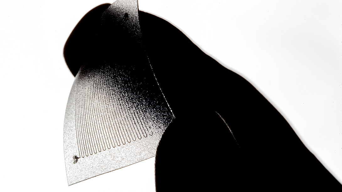
With the help of some microscopic canals, squishy materials and chemistry, Nebraska’s Stephen Morin is throwing a curve into the normally flat landscape of circuitry.
If a processor is the brain of a computing device, then circuits are the nerves that help power and direct its other major organs: sensors, transmitters, receivers. But unlike nerves, whose flexibility has allowed animals to evolve various body shapes and structures, circuits usually get confined to the flat, rigid surfaces of traditional circuit boards – which end up in similarly boxy devices.
By contrast, Morin and his team have developed a technique for painting circuits — typically copper — onto curved, textured and stretchable surfaces. The potential result: transforming almost any surface, even one normally relegated to protection or structural integrity, into a de facto circuit board.
That capability could save engineers valuable weight and space, expand the use of circuitry in limited-use products, give product designers unprecedented freedom, and help manufacturers reduce the use of materials, the researchers said.
“By doing this, you can create metallic traces on three-dimensional objects in a way that had not been possible before,” said Morin, assistant professor of chemistry at Nebraska.
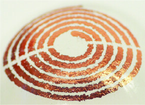
The technique itself is relatively simple, which Morin said should make it more affordable and accessible than existing alternatives. First, the team imprints microscopic canals – the circuit design – into an elastic material such as silicone. Compressing that patterned material against the desired surface — a cylinder, a sphere, a corrugated plane — creates a strong but reversible seal.
That seal allows the team to inject a solution through the canals, essentially seeding rows of microscopic particles. After removing the elastic overlay, the team bathes the surface in copper and a second solution, which reacts with the first to germinate the seed particles and chemically coat them with the copper. The metallic copper adheres only to the pathway defined by those seeds.
“What people in the industry have (traditionally) done is to use a laser to carve trenches on a three-dimensional object, then later deposit copper on it,” Morin said. “So you need a laser, and you need mechanical stages that move and position the part very precisely.
“From a simplicity standpoint and a cost standpoint, there are a lot of advantages to using the method that we’re reporting.”
Circuit gets the sphere
In a recent study, the team used its technique to deposit metallic traces for a light-sensing circuit onto a hemisphere, then showed that an LED connected to the circuit would light up when the sensor was covered. The researchers also deposited a radio-frequency antenna onto a cylindrical surface, demonstrating that a smartphone could read the antenna via near-field communication.
Taking better advantage of the many neglected surfaces in electronic devices could prove especially valuable when weight is at a premium, Morin said, with aerospace engineering among the most prominent examples.
“If you can remove the need for dedicated substrates to house electronic circuits by coating support elements with those circuits, then you can save material and mass,” Morin said. “So I think there are a lot of interesting potential applications there.”
Because saving material and simplifying production also saves money, the technique could expand the use of circuitry in applications far more pedestrian than jetting into the cosmos – especially the sorts of inexpensive electronics that generally have limited lifespans.
“The newest iPhones are $1,000,” Morin said. “If I have an expensive antenna inside of that device, who cares? But do you put a very expensive antenna in a toy to make it do something cool and interesting? No, because it’s not going to be compatible with the cost point and envisioned lifetime of the device.
“Whenever you can cut the cost of making something like a three-dimensional antenna, you can think of putting it into more affordable products, and you can augment those devices with functions that would normally be reserved for very expensive devices.”
Morin said the technique, which the team demonstrated on multiple types of plastics, could hypothetically open up the use of circuitry even in so-called consumables that are used only a few times. One potential example: Adding a simple antenna to the curved surface of a Solo cup would allow fans at crowded Huskers tailgates to identify their cup via a smartphone app in lieu of a Sharpie.
And freeing product designers from the rigid confines of the circuit board could lead to more organic, aesthetically pleasing designs in limited-use and long-term electronics alike, he said.
“I think it’s often dismissed how big of a role design actually plays in everyday life, but I think it’s really important,” Morin said. “Being alleviated from planar circuit boards and housing could really lead to some interesting (forms) in terms of our everyday objects.”
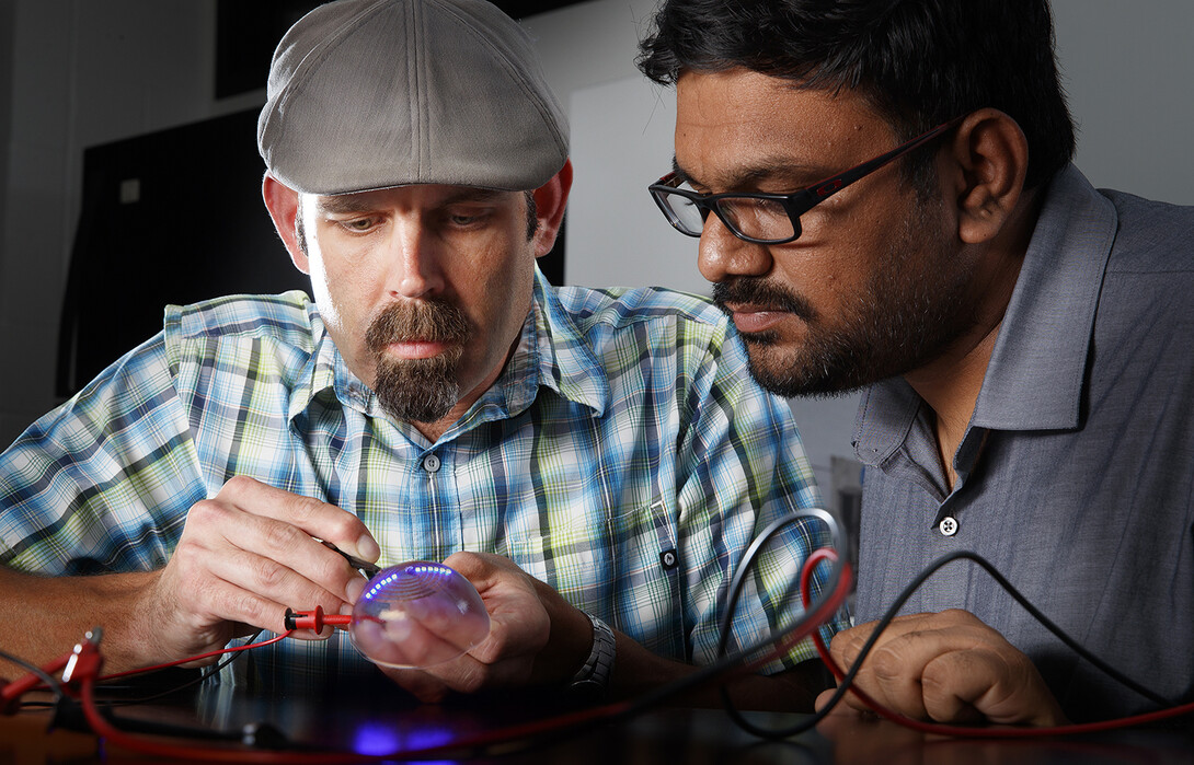
Morin’s team reported its technique in the journal Advanced Functional Materials. He authored the study with Abhiteja Konda, postdoctoral researcher in chemistry; Christos Argyropoulos, assistant professor of electrical and computer engineering; Advaith Rau, Michael Stoller and Jay Taylor, doctoral students in chemistry; Gabriel Pribil, freshman in computer science; and Purdue University’s Abdul Salam.
The team received support from the National Science Foundation and the Nebraska Research Initiative.