For years, researchers have been trying to find ways to grow an optimal nanowire, using crystals with perfectly aligned layers all along the wire.
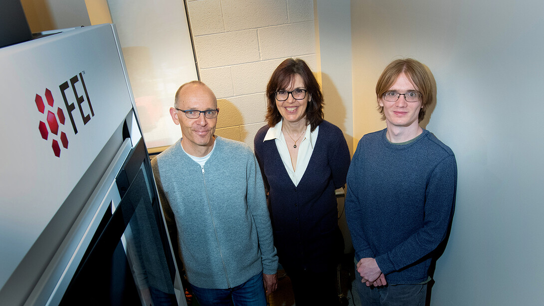
A team of Nebraska Engineering researchers — Peter Sutter, Eli Sutter and Shawn Wimer — sees an advantage to natural imperfection.
Through their research, highlighted in a letter published in the April 22 edition of the journal Nature, the group found that a defect — a screw dislocation — that occurs in the growth process causes the layers of crystals to rotate along an axis as they form. This defect creates twists that give these nanowires advantages, particularly in electronics and light emission.
“In layered nanowires, we basically have a new architecture that implements a crystal twist between two-dimensional materials,” said Peter Sutter, professor of electrical and computer engineering. “We take the approach that you can (either) make such twist moiré structures or have them make themselves, and when we let the wires do the job on their own, nature introduces this defect, a twist.”
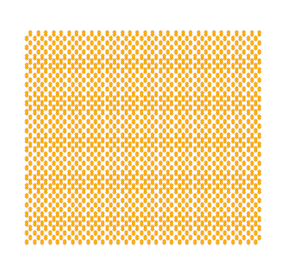
Typically, materials with twisted interfaces are artificially created from two atomically thin 2D crystals. When these crystals are painstakingly placed on top of each other, a small rotation among them — an interlayer twist — causes a moiré, or a beat pattern that changes with the twist angle and is much larger than the spacing of the atoms in the material. The motion of electrons in this beat pattern can cause new phenomena, such as superconductivity or systematic changes in the color of emitted light.
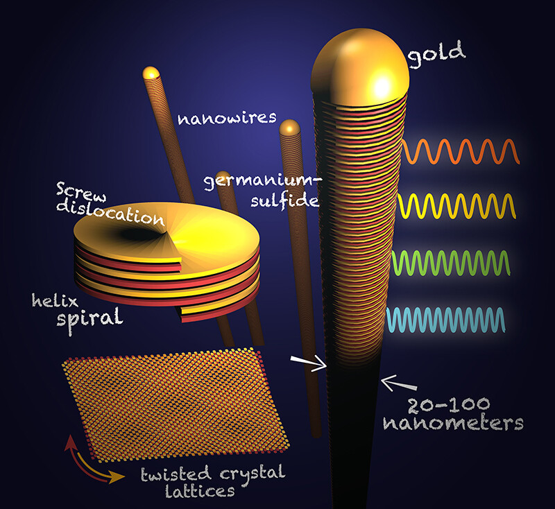
The Sutters’ team took a different approach to realizing these twists by growing nanowires that consist of 2D layers. They took small particles of gold, heated them up and inundated them with a vapor of germanium sulfide. At high temperatures, the gold particles melted and alloyed with the germanium sulfide.
“At some point, it gets saturated and can’t take any more of it in. Then it has a choice: don’t take in any more and let a film grow over it on the surface, or continue to try to absorb more,” said Eli Sutter, professor of mechanical and materials engineering. “It turns out these particles are greedy for germanium sulfide.”
The gold particles kept absorbing the vapor but became too saturated to hold it all and began growing layered crystals of germanium sulfide, one per gold particle. When the germanium sulfide was expelled, the crystals lengthened and turned into nanowires that are about 1,000 times thinner than a human hair.
The team discovered that each of these wires had a screw dislocation, which produced a helical structure and the twist between their crystal layers.
To explore the properties of their helical twisted nanowires, the team used a focused beam of electrons to stimulate the emission of light from minute portions of their nanowires. When the excited electrons relax, they emit light of a characteristic color or frequency, which the researchers recorded.
By allowing for an imperfect stack of twisted layers, the germanium sulfide nanowires emit different colors of light at different points along the wire. This makes it possible to tune the band gap and control the energy of absorbed or emitted light.
“We were able to show there are new, accessible light-emission properties that change along the wire because the moiré registry changes,” Eli Sutter said.
Twisted nanowires of germanium sulfide, a semiconductor, could have applications that include energy harvesting, tunable light sources, or next-generation computing.
The researchers, however, said their next step is understanding why the color of emitted light changes along the wire and possibly achieving similar results with other materials.
“We have to better understand the consequences of the helical twist structure. We expect that twisted nanowires still have many other surprises in store for us,” Peter Sutter said.
This material is based upon work supported by the National Science Foundation under Grant No. DMR-1607795. Any opinions, findings, and conclusions or recommendations expressed in this material are those of the author(s) and do not necessarily reflect the views of the National Science Foundation.
The development of advanced experimental techniques and of associated data analysis methods enabling this work was supported by the U.S. Department of Energy, Office of Science, Basic Energy Sciences, under Award No. DE-SC0016343.